usb3sun rev A1, a usb input adapter for sun workstations
SPARCstations have a unique serial-like interface for keyboard and mouse input, using a single 8-pin mini-din port. usb3sun allows you to use an ordinary USB keyboard and mouse with your sun workstation!
back in january, i wrote about the prototype version we (+na) built to get our SPARCstations up and running, when we only had a keyboard but no compatible mouse. that worked well enough, and i even wrote a guide to building one yourself, but it wasn’t really accessible to anyone other than the most dedicated hobbyists.
since then, i’ve learned how to design a pcb, turning usb3sun from a hack into something more polished. want to know more? here’s another 5600 words about this project, plus what i learned about robust electronics, drawing schematics, designing a pcb, and 3d printing!
toc
- requirements
- schematic
- pcb layout
- dual power
- doing usb correctly
- protection features
- rev A0
- rev A1
- supporting the display
- next steps
requirements
the basic requirements of the breadboard prototype are more or less unchanged.
the adapter communicates with the workstation over serial, and needs to act as a usb host for the keyboard and mouse, providing a 5V supply to each.
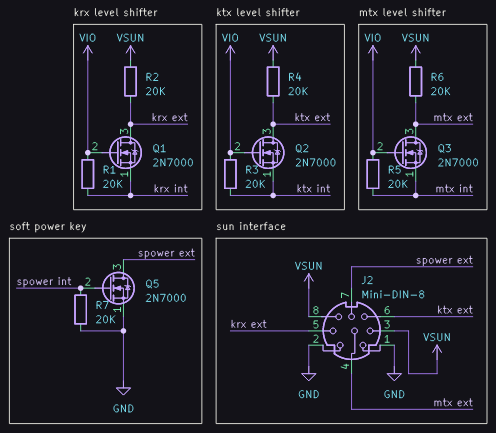
we need to power the adapter and the usb devices somehow, and we can get a 5V supply from either the workstation itself or an external debugger, but sadly the 5V pin on the sun interface is only powered once the machine is on.
newer sun keyboards (starting with sun type 5) also have a power key, which turns the workstation on, in addition to sending make and break codes like other keys. on those keyboards, the power key is wired to pull the power pin (SPOWER below) to ground, but on a usb keyboard, we can’t detect any key presses without some way of powering the keyboard.
this means we can only emulate the “soft” power key when the adapter is powered externally, but a “hard” power key that uses a button on the board itself will work at any time.
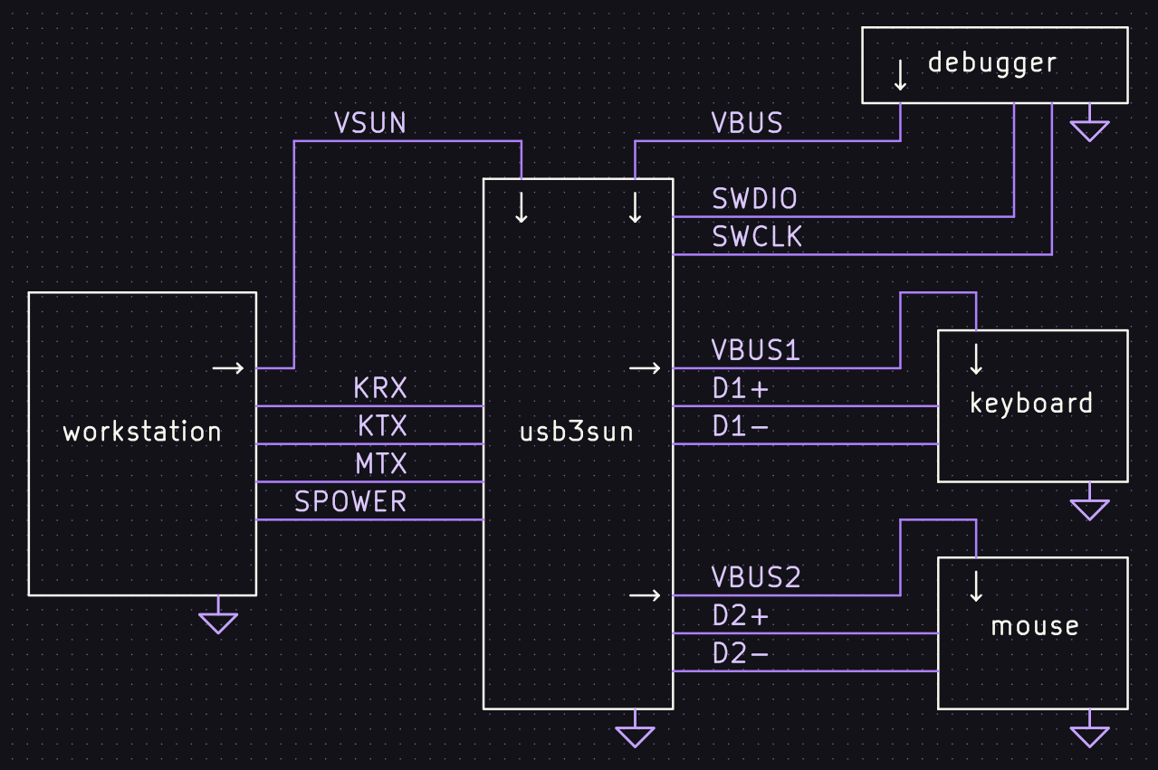
one new requirement is that we use the 5V supply from the sun interface where possible (§ dual power). in the prototype, i ignored this supply since i always had an external debugger or usb charger nearby, but it doesn’t really make sense to expect everyone to use an external power supply unless they need it for the “soft” power key.
since this is no longer a prototype, there are also things we needed to do for correctness and robustness, but more on that in § doing usb correctly and § protection features.
my initial
schematic
was a direct translation from paper to computer.
mistakes aside, i soon learned a few other lessons.
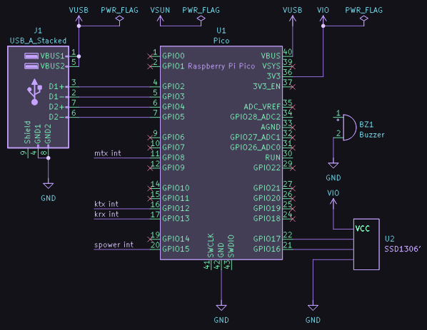
when drawing schematics, symbols can (and should) diverge from the physical pin layout where it would improve readability. if you don’t like the symbol you got from (say) snapeda, you can modify it or even draw your own!
the general convention for schematics is to use capital letters and underscores (no spaces) for net labels, and ensure all pins and wires are snapped to the 0.1″ grid. notably, this means you should always use R_Small, not R.
if you’re using kicad and sending your boards to jlcpcb like me, install jlcpcb tools. it’s a great plugin that lets you look up parts in jlcpcb’s database, save part numbers and component rotations to your schematic (though this feature seems to be broken), and generate your gerbers and other files in the correct format.
here are some other lessons i learned about
pcb layout
!
you should familiarise yourself with the behaviour of the “electrical rules checker”, “design rules checker”, “update pcb from schematic”, and symbol/footprint library features. playing around with them and understanding how they work will save you time in the long run.
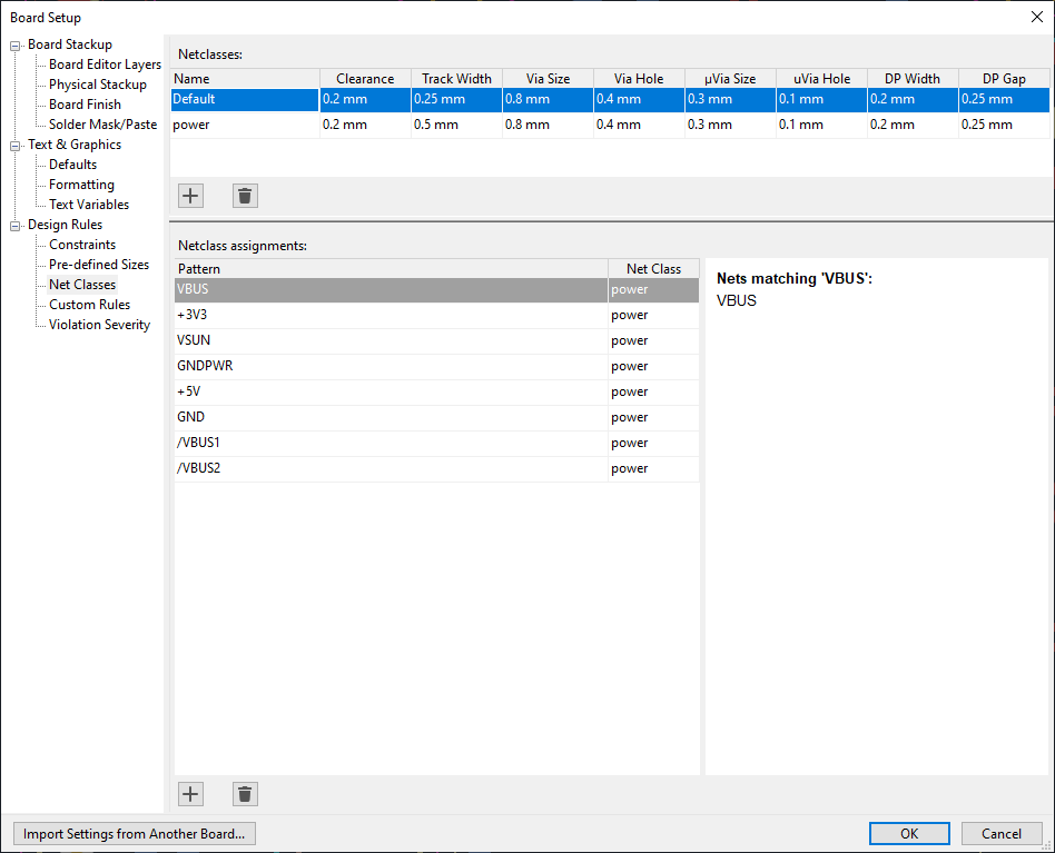
always set up your stackup, constraints, and netclasses before you start drawing any traces. i used these settings for jlcpcb based on their pcb capabilities and pcb assembly capabilities:
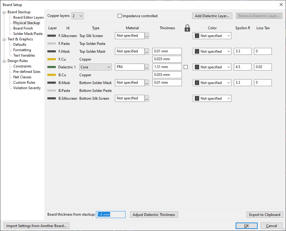
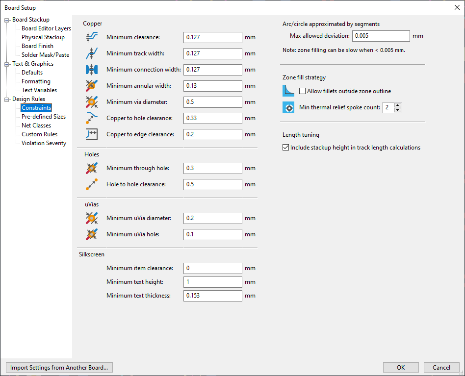
power supply traces that carry a lot of current need to be wider, to reduce their resistance and in turn compensate for the increases in voltage drop and heat dissipation.
according to this calculator, even with jlcpcb’s allegedly thinner traces of as low as 28.25 μm, we can pull up to 750mA over a 0.25 mm trace or 1230mA over 0.5 mm with only 10 °C temperature increase, and the voltage drops per inch are also acceptable for our small board.
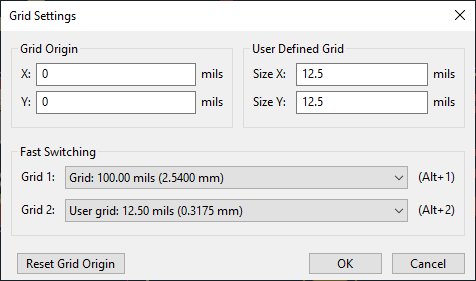
unlike schematics, pcb layouts don’t need to be aligned to a 0.1″ grid, and limiting yourself to that can make it impossible to place and route small SMT components cleanly. so despite making the board size a multiple of 0.1″ (100 mils), i laid everything out on a grid of 12.5 mils.
kicad 7 was released just as i started designing these boards. talk about good timing! two new features that i found useful for the pcb layout are “pack and move footprints” and native support for teardrops.
“pack and move footprints” helps with laying out components in high-level functional groups, which is especially valuable when you’re just starting a layout and all of the footprints are in one big pile. if you select some symbols in the schematic and switch to the pcb editor, their footprints will also be selected, and you can press P to gather them up and move them together as a group.

kicad can add teardrops! teardrops are a neat feature that can improve structural integrity under thermal and mechanical stress, make your pcb easier to manufacture successfully, and most importantly they look cooler.
there’s a small footgun to this though. “add teardrops”, “remove teardrops”, and “fill all zones” are all imperative operations, so you need to remember to fill all zones after you add or remove teardrops, just like you needed to after drawing any traces. otherwise you can end up with zones that get too close to traces or vias, like the copper fill shown here in magenta.
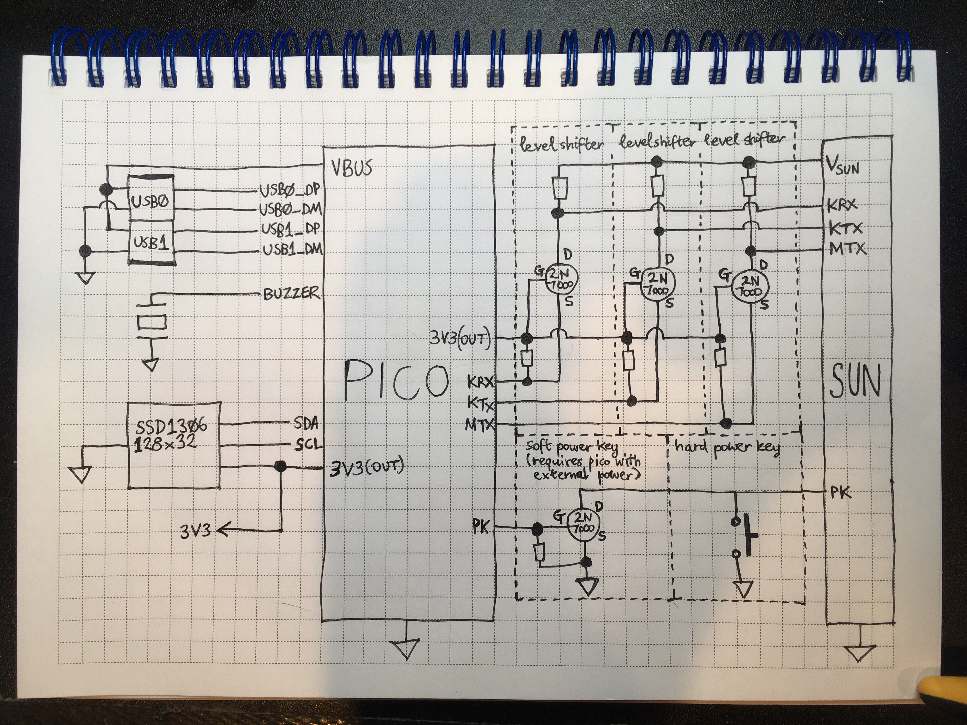
dual power
according to the pico datasheet (§ Powering Pico), we can power a pico with anything between 1V8 and 5V5, so here’s what we know:
- we have
- 5V supply from VBUS (when charger or dev machine connected)
- or 5V supply from VSUN (when workstation powered on)
- we need
- 5V supply to pico (or at least 1V8)
- and 5V supply to usb host ports
“ORing” two power supplies is a bit more involved than just bridging them together, because when both power supplies are connected, we need to isolate them from one another to prevent backfeeding. both VBUS and VSUN are nominally 5V, but let’s say in reality VBUS was 4V9 and VSUN was 5V2. if they were bridged together, then the 0V3 potential difference would mean current would flow from VSUN into VBUS, which would be pretty rude and potentially damage the device providing VBUS.
the problem with ORing circuits is that there’s always some voltage drop. this wastes energy as heat and can eat into our voltage tolerances, creating problems if the output needs to be the same voltage as the inputs. that said, we can minimise this drop to the point where we have something that works well enough.
here are the three approaches we tried. the first two were stolen directly from the pico datasheet’s examples of how to supply VSYS from VBUS or an external supply. note that in those examples, the pico provides the diode from VBUS to VSYS, but in our case, to keep things consistent between approaches, we’ll provide our own diode and connect the output directly to VSYS.
two schottky diodes
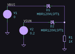
the simplest power ORing circuit is to put each power supply behind a diode. this blocks current in the reverse direction at the expense of a voltage drop, known as the forward voltage, and we can minimise this voltage by using a schottky diode.
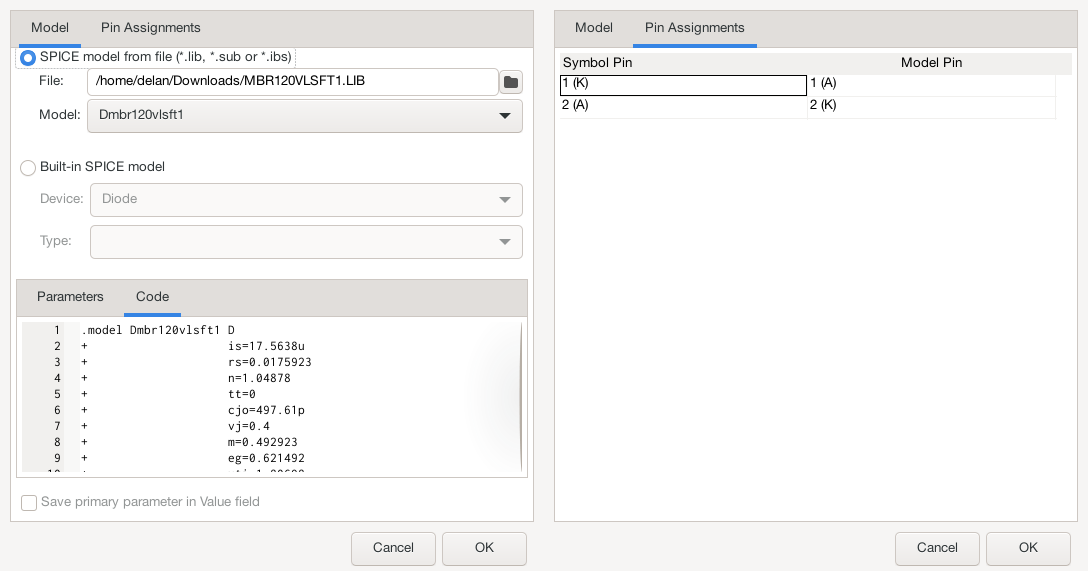
according to its datasheet, the MBR120VLSFT1 can block up to 20V of reverse voltage at the expense of a 0V34 voltage drop, and even if one diode’s input was at 0V and the output side was at 20V, only 15mA would leak back into the 0V supply.
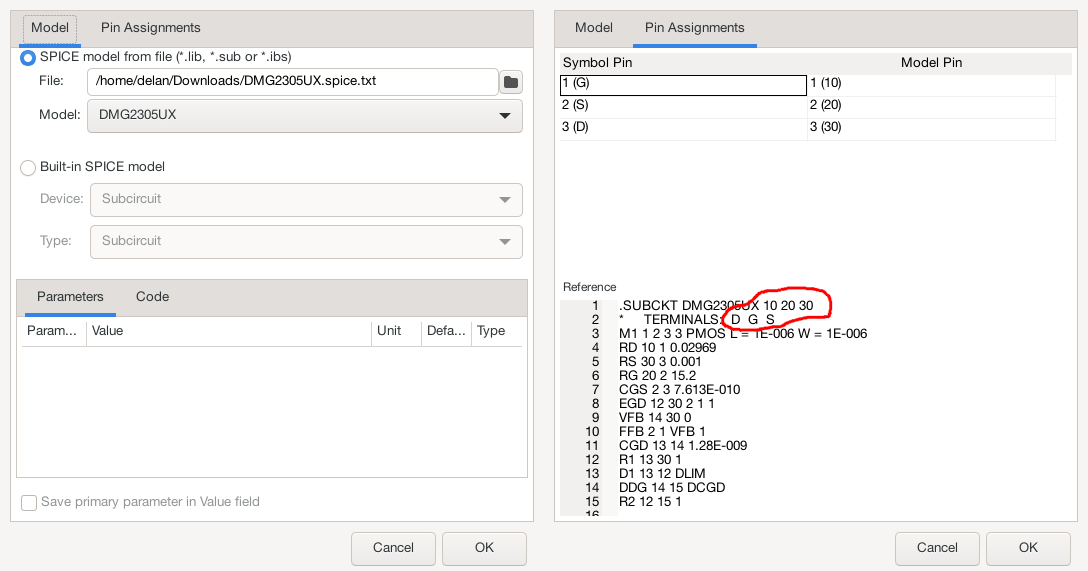
we can simulate this circuit in kicad to see how the output voltage behaves at different combinations of VBUS and VSUN, by setting up the Sim Command as a DC Transfer with two sources. to get realistic results, we need to give kicad a spice model for our diodes, which we can find on the web by searching for “MBR120VLSFT1 spice model”. there are a few things to watch out for:
-
Source 1 gets used as the x axis, so the increment step can and should be small, but Source 2 creates separate signals (coloured lines), so a small increment step will result in many lines that will each need to be double-clicked if you want to remove them from the plot
-
kicad will crash if you forget to assign a model to any of the symbols in your schematic, so you’ll want to run simulations against a minimal circuit that only has the relevant components
-
if you use a non-spice diode symbol (read: anything outside the Simulation_SPICE library), the pins will be numbered “wrong” by default, because kicad symbol libraries use the ipc convention where pin 1 is cathode (K), but spice uses a convention where pin 1 is anode (A)
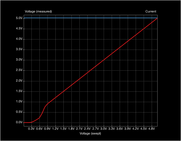
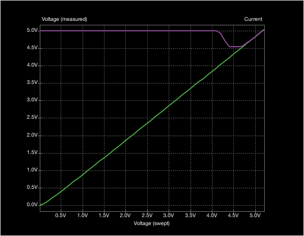
here we can see that when either of the inputs are 5V, the output will be around 4V8, and in general the output voltage is around max(VBUS,VSUN)−0V2.
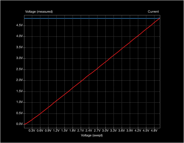
blue is VBUS sweep 0 to 5V when VSUN is 5V
green is VSUN sweep 0 to 5V when VBUS is 0V
purple is VSUN sweep 0 to 5V when VBUS is 5V
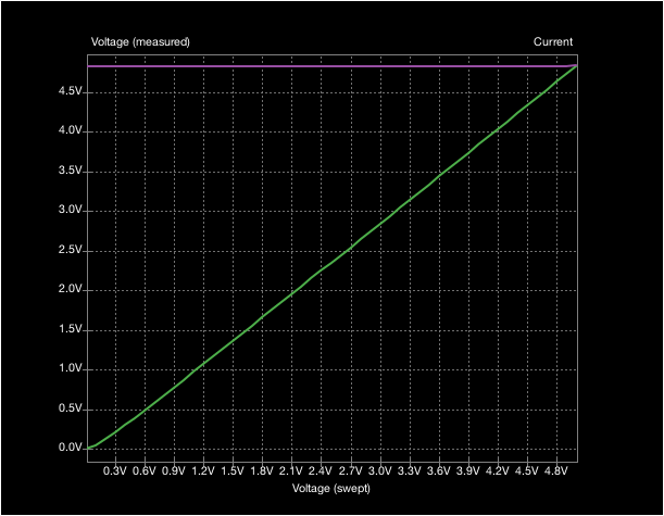
one schottky, one mosfet
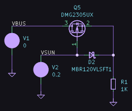
if we replace one of the schottky diodes with a p-channel enhancement mosfet, we can eliminate the voltage drop on that input when the mosfet is “on”, which happens when the gate voltage is far enough below the source voltage. this minimum potential difference is known as the threshold voltage (VGS(th) or Vt).
according to its datasheet, the threshold voltage of the DMG2305UX is between −0V5 to −0V9. this is only an indication of when the mosfet will start turning on, in this case just enough for −250µA to flow through the drain. not an indication of when it will be fully on.
i measured actual voltages of VSUN and VBUS on borealis (SPARCstation 5) and a variety of usb chargers and ports. VSUN was 5V2, while VBUS was generally between 5V0 and 5V1, so i decided VBUS needed the mosfet more.
we can simulate this circuit, and just like before, if you use a non-spice mosfet symbol (read: anything outside the Simulation_SPICE library), the pins will be numbered “wrong” by default, because kicad symbol libraries use the ipc convention where pins 1-2-3 are gate-source-drain (G-S-D), but spice uses a convention where pins 1-2-3 are drain-gate-source (D-G-S).
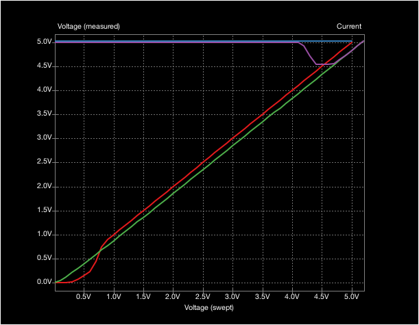
here we can see that when VSUN is zero (red), the output will equal VBUS as long as VBUS is at least 0V9, and when VBUS is zero (green), the output will be around VSUN−0V2, but when VBUS is 5V (purple), the output drops below VBUS as VSUN reaches 4V1 and stays that way until VSUN reaches 5V2.
blue is VBUS sweep 0 to 5V when VSUN is 5V2
green is VSUN sweep 0 to 5V2 when VBUS is 0V
purple is VSUN sweep 0 to 5V2 when VBUS is 5V
let’s look at why the output changes so much when VBUS is held at 5V:
- when VSUN is zero, the mosfet is on, allowing current to flow from drain (VBUS) to source (output) without any voltage drop, so the output is 5V00
- at 4V1 (VBUS − VGS(th)), the mosfet starts turning off
- at 4V4, the mosfet is off, and VBUS can only flow to the output via the mosfet’s body diode, which has a voltage drop of ~0V45, so the output is 4V55
- at 4V7, the schottky diode has a voltage drop of ~0V15, and its cathode reaches the same voltage as the output
- beyond 4V7, the output is controlled by the schottky diode, so VSUN is now the effective power source
these simulations were all done with R1 at 1kΩ, which at 5V is only 5mA. if we used a more realistic current of say 200mA (25Ω), the output voltage drops by as much as 0V6 when VSUN is close to VBUS. at a more extreme current of 1A (5Ω), it drops by as much as 0V7, and we even start to see up to 0V1 voltage drop while the mosfet is on due to its RDS(on)!
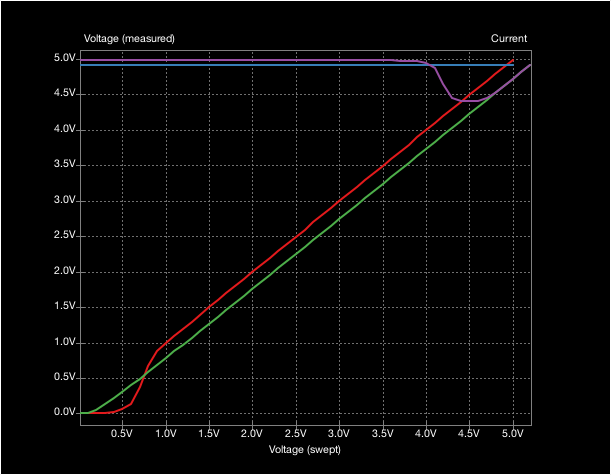
red is VBUS sweep 0 to 5V when VSUN is 0V
blue is VBUS sweep 0 to 5V when VSUN is 5V2
green is VSUN sweep 0 to 5V2 when VBUS is 0V
purple is VSUN sweep 0 to 5V2 when VBUS is 5V
ultimately it’s not a great idea to rely on the favourable characteristics of one particular workstation. instead we want to maximise our performance under nominal voltages and tolerances.
“ideal” diode
we can do even better than this by using an “ideal diode” like the MAX40200. these are designed to be used like a schottky diode for ORing, but are actually a mosfet with a comparator under the hood. this is related to active rectification, which is pretty much the same technique applied to AC-to-DC conversion.
as long as the load current is reasonably low, the voltage drop of a mosfet (Iload × RDS(on)) can be lower than the (roughly stable) voltage drop of a schottky diode. this also improves efficiency at low voltages, because a schottky diode that drops 0V3 at 5V is a 6% loss.
you can learn more about ideal diodes in this 25-page paper by texas instruments.
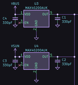
per the datasheet, we need at least a 330pF capacitor on the input and at least a 330pF capacitor on the output.
i wasn’t able to get the vendor’s simulation model to work in the spice that comes with kicad, but we should still be ok to use it as long as we read the datasheet carefully like we would for any component.
doing usb correctly
replacing our gpio-based usb host ports with otg-based ports that use the rp2040’s native usb hardware might make our usb support more reliable, but there are two issues that affect our design either way, at least in terms of compliance.
one is the
power supply
.
usb host ports, including the ports on usb3sun, need to supply a VBUS between 4V75 and 5V50. our power supply design means that the input we receive from a workstation or external debugger needs to be at least 4V75 plus the voltage drop of our ideal diodes, which can be up to 175mV at 1A.
in theory, our host ports would be non-compliant if we expose the micro-usb port in a future revision (§ next steps) without any other changes, because then we could be a usb device when powered externally. and as a device, we can only expect 4V375 on our upstream VBUS, or 4V625 if we have permission to draw 500mA. oh yeah, did you know usb devices are supposed to ask before drawing more than 100mA?
to be honest, i think our host ports are already non-compliant. for example, the sparc keyboard spec doesn’t define the voltage and current limits of its +5V pins, and without any limits, we have no way of knowing whether +5V is at least *tap tap tap* 4V925.
afaict the only way to make them compliant is to replace the ideal diodes with a proper voltage regulator that can boost the input if necessary, but i’m also not sure this matters too much in practice.
the other is
signal integrity
.
on the spectrum of performance and complexity from like… serial to pcie, usb is somewhere in the middle. usb 2.0 can be kinda fast and kinda tricky to get right, but it’s generally not too difficult.
the usb data lines are a differential pair, which for reasons beyond my understanding need to be routed carefully. generally this involves:
- terminating the two traces with a pair of series resistors
- minimising the distance between the two traces
- minimising the difference in length between the traces
- surrounding the traces with ground planes in xy or z directions
this is very important for high speed usb, but our host ports only support low speed and full speed, so this probably doesn’t matter too much. that said, i did my best to route the pairs as if we needed to support high speed, if only to learn how to do it.
i used kicad’s “route differential pairs” (6) tool for this, and it worked well enough once i started holding Ctrl to disable grid snapping at all times. when grid snapping is enabled, kicad tries to ensure that the destination under your cursor is both aligned to the grid and satisfies the differential pair routing rules, and the intersection between these sets of points is often zero.
you can learn more about routing usb in this post (and video) by zachariah peterson, or this video by cole brinsfield:
https://www.youtube.com/watch?v=aAqJYWu5Y8c
protection features
unlike the breadboard prototype, the pcb versions of usb3sun have components that protect against excessive current draw, both during normal operation and during a fault, plus electrostatic discharge and electromagnetic interference.
bypass capacitor
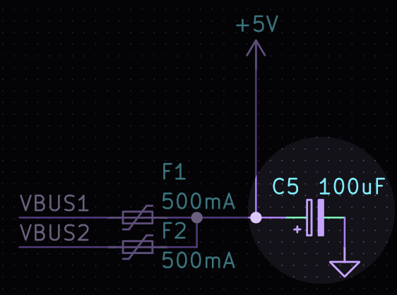
excessive current draw during normal operation can cause the power supply voltage to drop, which can negatively affect other components that depend on that rail.
putting a 100uF bypass capacitor on +5V, parallel to (and near) the trace that feeds VBUS1 and VBUS2, allows devices connected to the usb ports to satisfy brief spikes in their current draw without disturbing the voltage of the +5V rail, since they can instead draw most of that current from the capacitor.
the flipside of this is that the capacitor needs to draw current to charge itself, which can create a spike in current draw when initially powering up the adapter.
you can learn more about this in the usb 2.0 spec (usb_20.pdf § 7.2.4.1).
overcurrent protection
excessive current draw during an electrical fault can damage power supply traces and other components like the current switches (ideal diodes). this can happen if a device connected to one of the usb ports malfunctions, which is probably rare, but it can also happen in more likely situations, like a misplaced screwdriver in one of the usb ports shorting its VBUS{1,2} to ground.
to protect them against this, we use two polyfuses, one on VBUS1 and one on VBUS2, that are each guaranteed to trip at ≥1A (the trip current) and guaranteed not to trip at ≤500mA (the hold current). the latter value is notable for usb, because ordinary usb devices are not permitted to draw more than 500mA at any time.
unlike an ordinary fuse, polyfuses generally don’t need to be replaced when they trip, though they can take a long time to fully reset back to their original resistance (if at all).
esd protection
electrostatic discharge can induce voltages far beyond the limits of many of the components, such as our ideal diodes which are only rated to 6V. to protect our circuit against this, we need esd protection diodes.
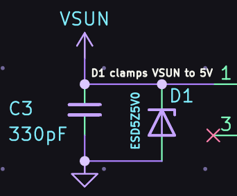
for the sun interface, we use the ESD5Z5V0, a tvs diode that protects VSUN by shunting any excess voltage beyond 6V to ground. this tvs diode is unidirectional though, so it won’t protect VSUN against negative voltages, and for now we haven’t protected the data lines.
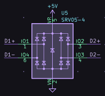
for the usb interfaces, we use the SRV05-4, which protects VBUS and the four data lines by combining a tvs diode with four pairs of steering diodes. the tvs diode protects VBUS unidirectionally, the lower steering diodes shunt negative ESD voltages to ground, and the upper steering diodes shunt positive ESD voltages to VBUS, which may in turn get shunted to ground via the tvs diode.
emi protection

to protect the usb ports from high-frequency electromagnetic interference on the order of 100 MHz, we use a ferrite bead (GZ2012D601TF) between the shield and ground.
unlike the other protection features, i don’t understand this one too well, and it was also unclear to me what the best practices are for emi protection on usb ports, so i borrowed the approach used here from the unified daughterboard, another keyboard-related usb hardware design.
you can learn more about emi protection for usb hardware in this 19-page paper by intel. notably it seems the best practices vary depending on whether you’re running at low speed or full speed, whether you are a host or device or hub, and whether you have a board-mounted receptacle or a captive cable.
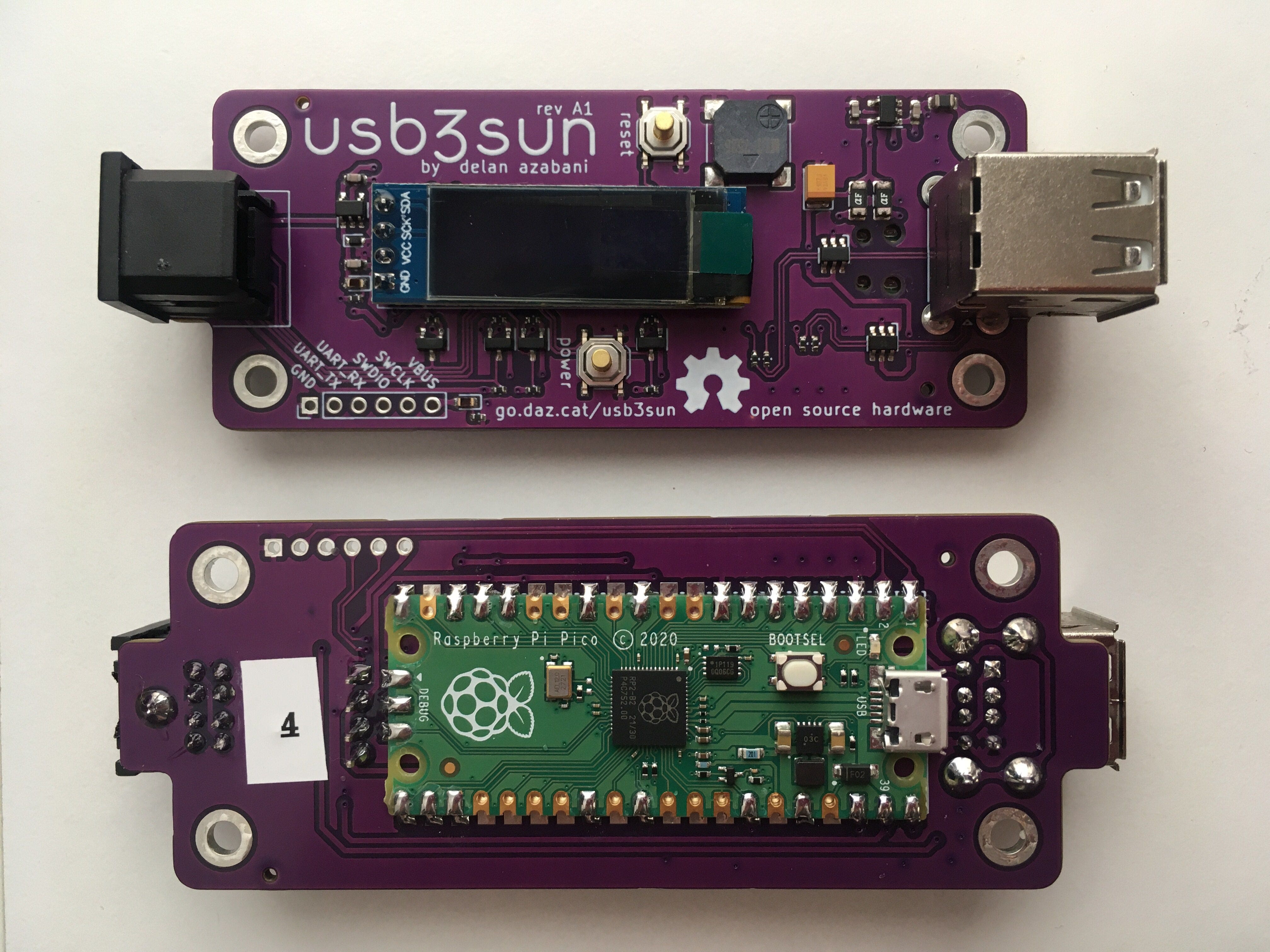
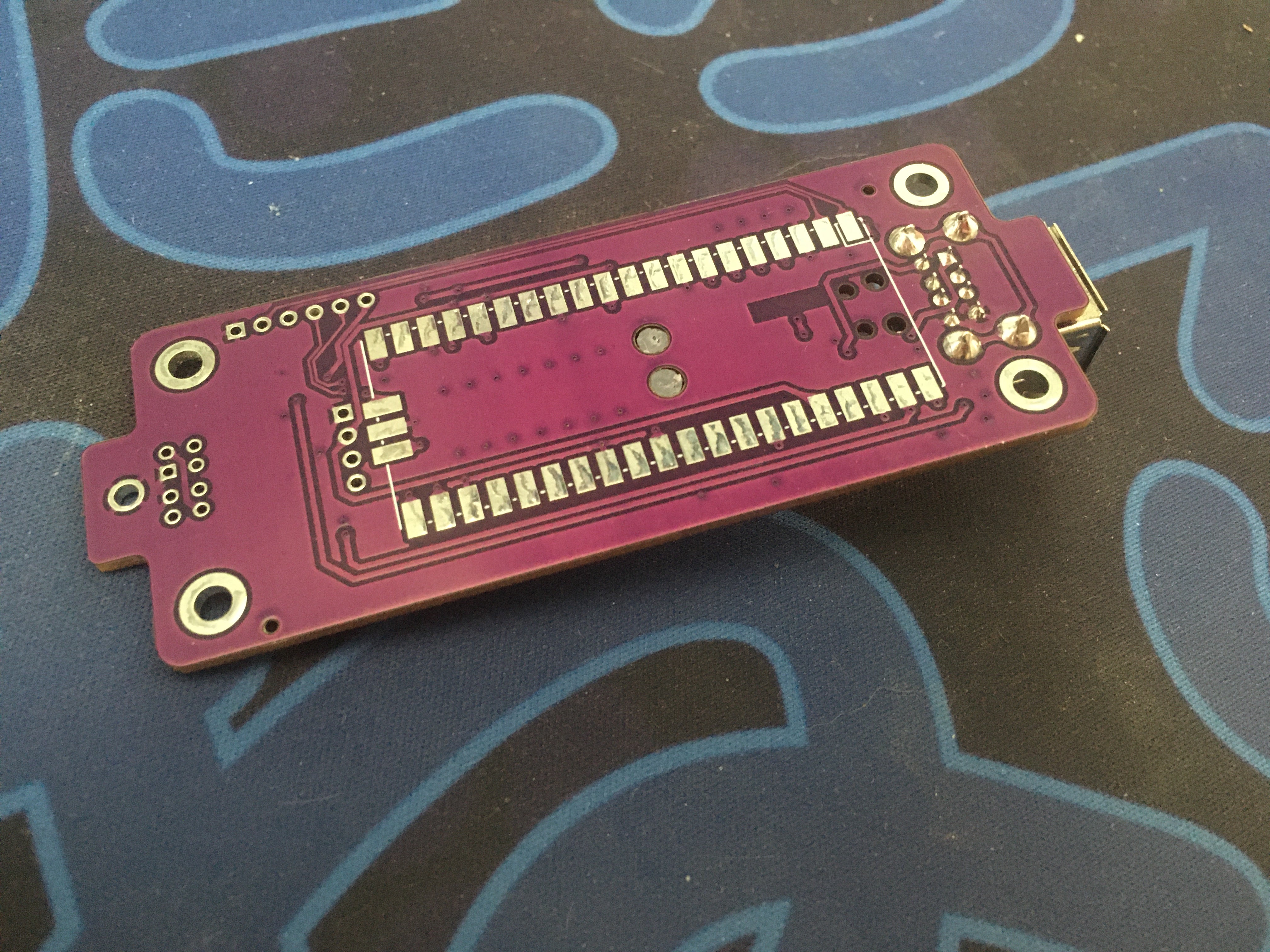
rev A0
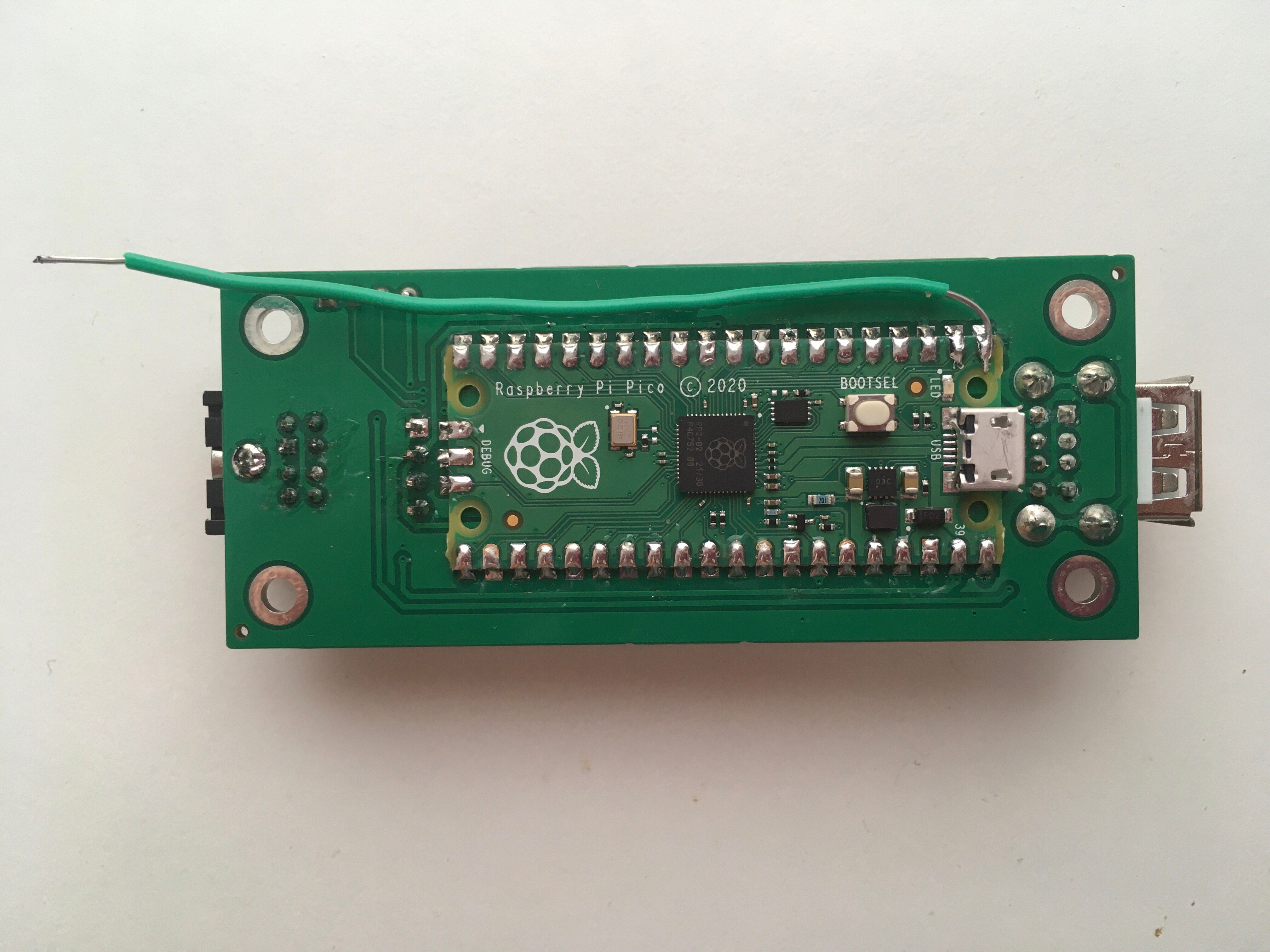
i sent rev A0 to the board house and it worked perfectly! the design was correct to the best of my ability, so this wasn’t unexpected, but the first revision is always nerve-wracking, more so when it’s your first ever pcb design.
the improvement in ergonomics by moving from the breadboard prototype to a proper pcb cannot be overstated. with the breadboard, wires would come unplugged all the time. this can be scary when it’s ground and an external debugger is attached, because i’ve seen potential differences of as much as 55V between the two power supplies when that happens.
that said, the usb host ports didn’t work at first. and with the usb stack we’re using, it really helps to have access to UART0 for debug logging, but i forgot to expose pins for that anywhere, so i had to solder a bodge wire. more on that in § usb shenanigans.
this design uses the same kind of four-pin module for the oled display as the prototype, which you can find countless clones of on aliexpress under “ssd1306 0.91”. this is easier to solder by hand than the eight-pin flexible ribbon version, which is important since jlcpcb doesn’t stock either of them (so they can’t assemble it for us).
there was nothing to support the end of the module opposite the header though, which makes the board unnecessarily fragile. i haven’t tried, but i think a misplaced finger could easily snap the solder joints, and potentially even rip the pads off the board.
usb shenanigans
debugging the usb stack was tricky. for one, attaching a debugger affects timing, which can make downstream devices appear to disconnect. and any upstream usb connection would use the same usb stack, so you can’t use the usb-cdc-based serial console for debug logging, since that would be a circular dependency.
as a differential diagnosis, i uploaded the same firmware i was using for testing to my (known good) breadboard prototype, and the usb ports stopped working there too. armed with the suspicion that it was the firmware’s fault, i found that the new firmware, built over three months later, used updated dependencies that led to some regressions.
one of them was that for reasons that are not yet clear, we stopped getting hid-related callbacks from the usb stack. the other was partially our fault. we had a workaround for a bug that was fixed upstream, and the workaround and the fix did pretty much the same thing. that thing wasn’t idempotent though, and doing it twice causes a panic.
i think the takeaway here is that you should always pin your dependencies to avoid unexpected regressions (and make builds more reproducible). this is currently easier said than done, so for now we only pin our direct and/or usb-related dependencies.
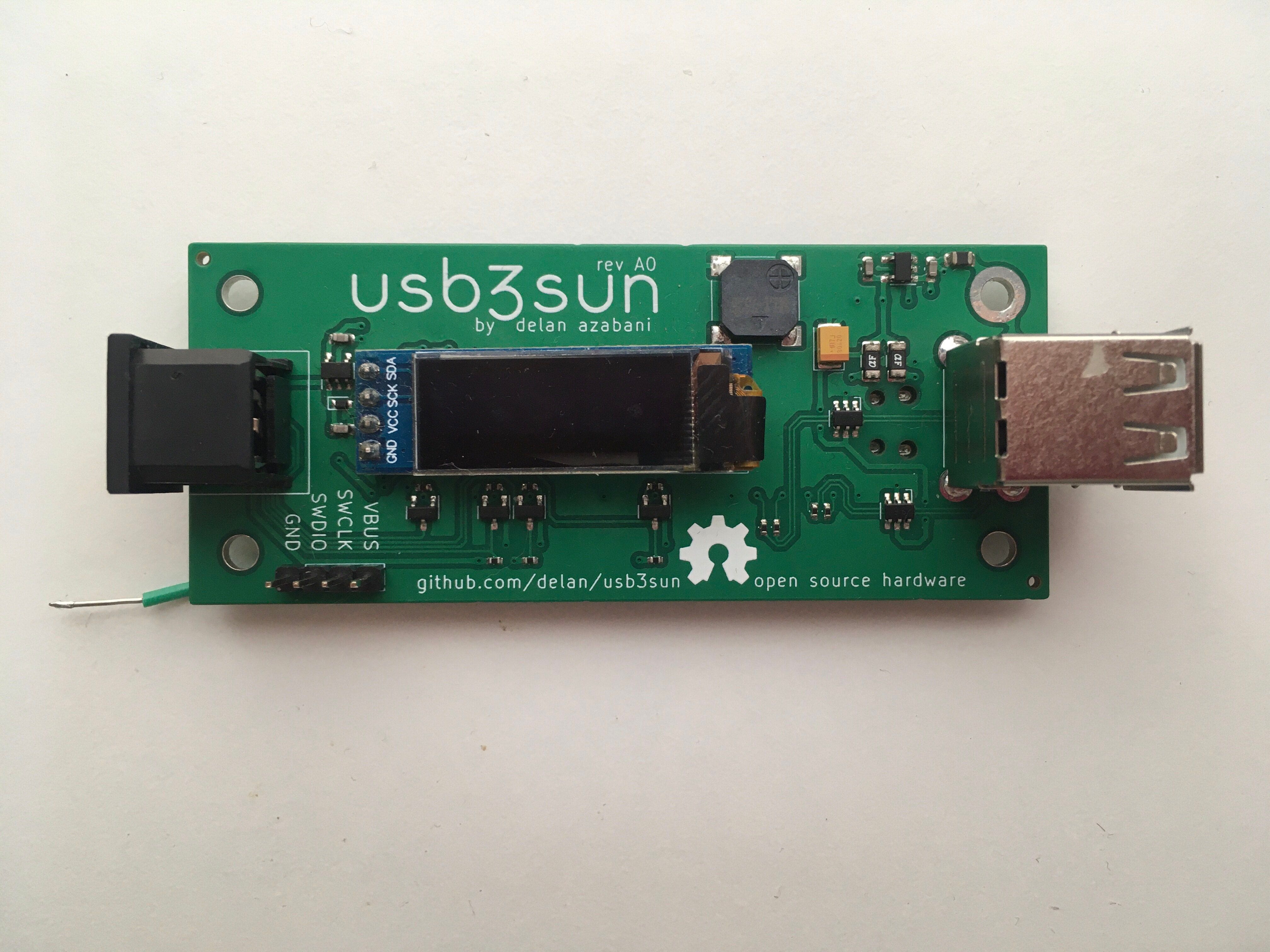
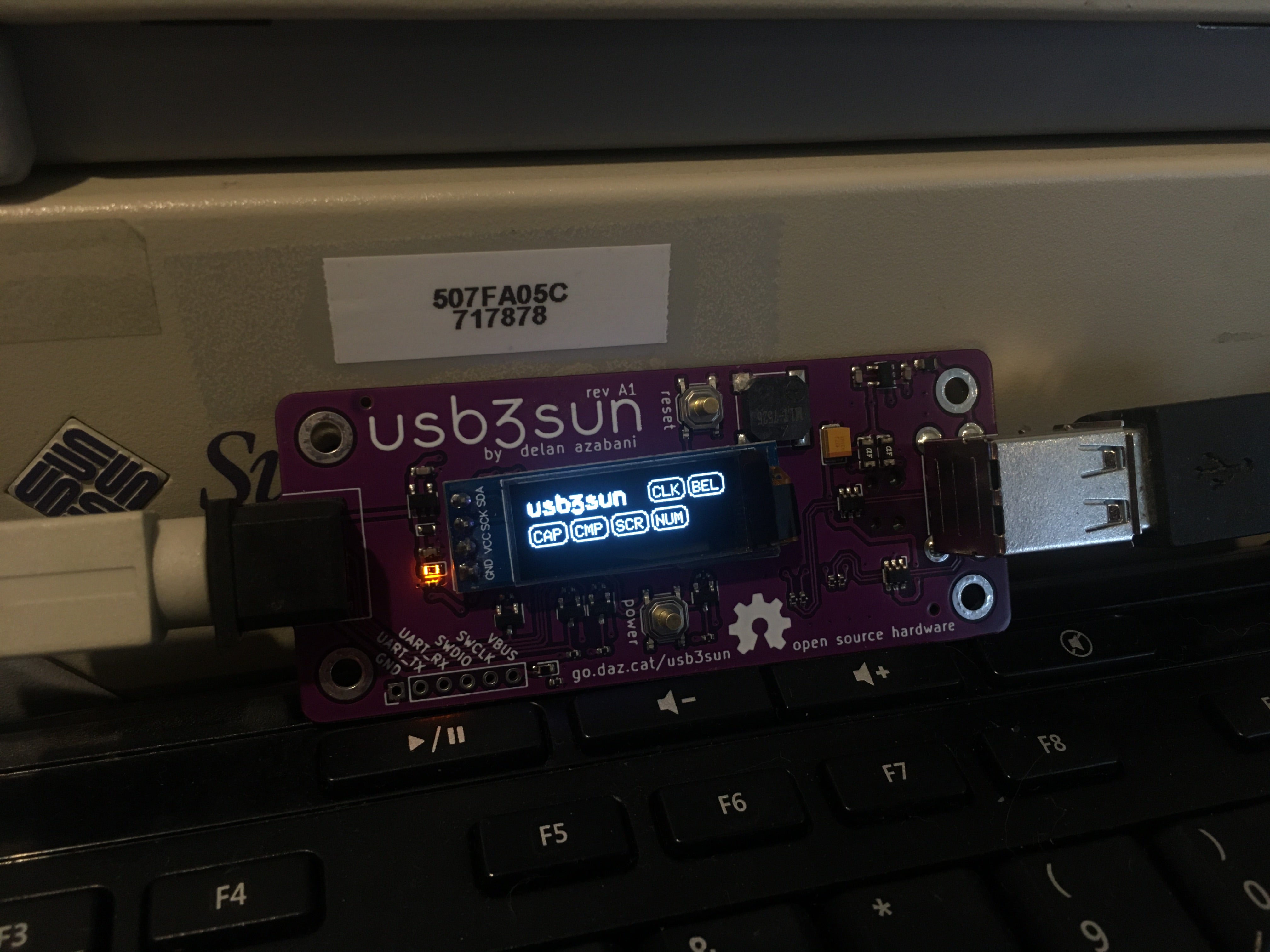
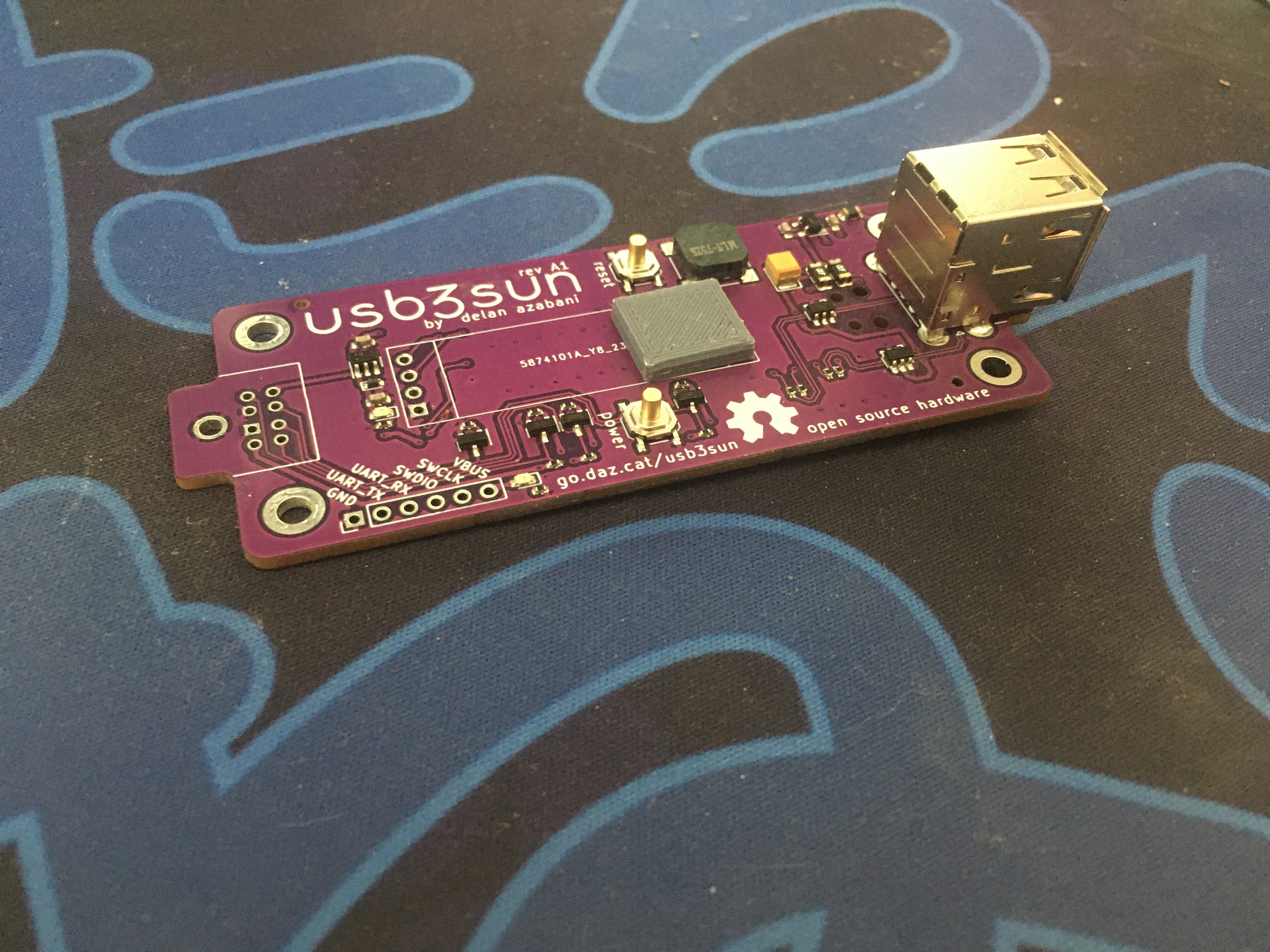
rev A1
the next (and current) revision fixes most of the shortcomings of rev A0, adding debug header pins for UART0, a 3d printed support to prop up the display module (§ supporting the display), and tactile switches for reset and “hard” power key.
rev A1 also polishes the pcb layout in a bunch of ways:
- the ground planes are now better stitched with vias, beyond the rule of thumb of “one via next to each ground pad”, to minimise ground plane islands
- the mini-din connector now sticks out of the board a bit like the usb connector, to make a future enclosure design more viable
- the corners of the pcb are now rounded, to make the board more comfortable to hold
- all of the corner mounting holes are now padded on both sides, rather than just the one connected to GNDPWR, which looks a bit nicer
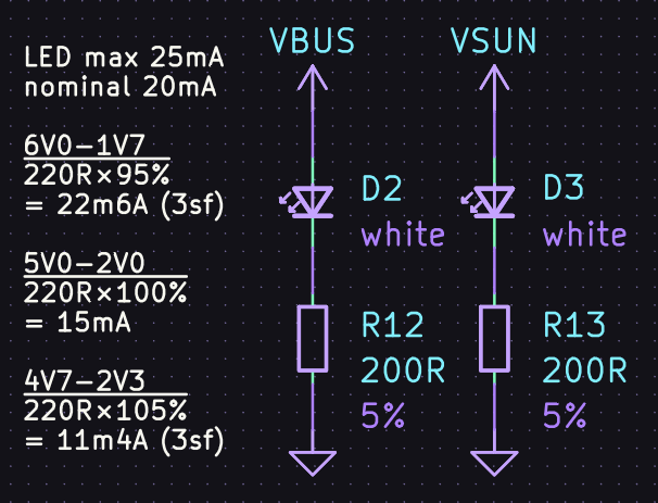
@ariashark also suggested i add some led indicators to check the state of the two input power supplies, independent of whether the firmware is running. i have two opinions about leds, which are closely related:
- most leds on consumer electronics are too bright
- blue leds are the spawn of satan (derogatory)
i picked the elegantly named 19-213/Y2C-CQ2R2L/3T(CY), a yellow led, in the hope that heeding the latter would also take care of the former. leds need their current limited externally or they will be damaged, and their brightness increases when the current increases. based on the nominal and maximum current ratings, i chose a resistor value that would yield 15mA normally and 23mA in the worst case.
i regret to inform you, my dear reader, that yellow leds can still be too bright. 0402 resistors are too small for me to swap out by hand, but i fixed the overwhelming brightness of the leds by blacking out the top of the packages with a marker.
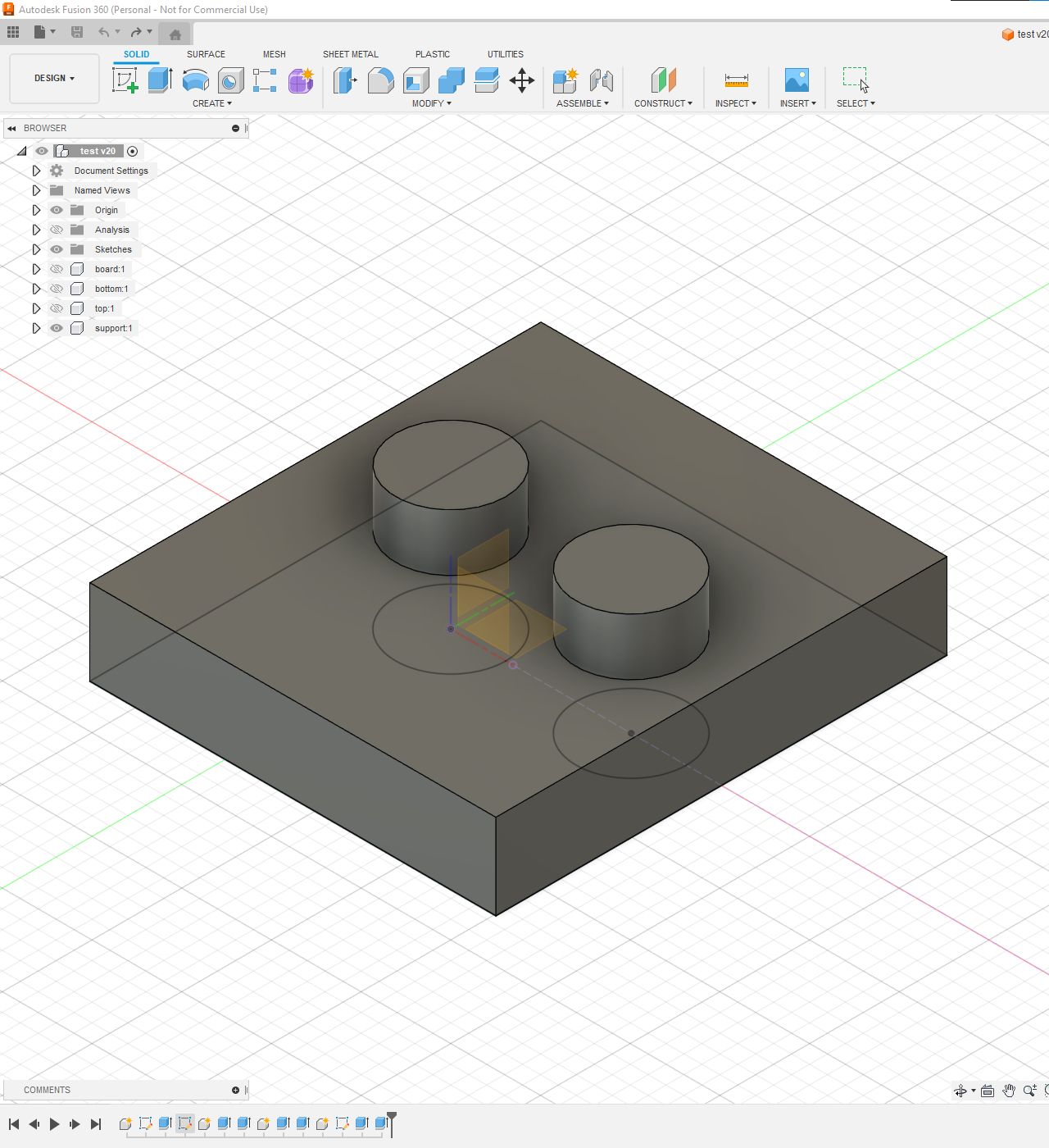
supporting the display
rev A1 adds two mounting holes under the display module to hold some kind of support. since @ariashark had recently set up our new 3d printer, this was a great time to design and print my very first model.
at first i thought i would need to make the support clip into the pcb. i decided to go with simple cylindrical posts, because it needs to be flush with the bottom of the pcb, and besides, there’s no real way it can fall out once the display module is assembled.
i ended up drawing the model twice, once in fusion 360 and once in freecad. fusion 360 is apparently what most people use to draw 3d printing models, but i honestly kinda hated it, and i would argue it detracts from the open-source-hardwareness of usb3sun. both models printed equally well, but i only bothered pushing the freecad model to github.
my first experience with
fusion 360
was being forced to create an account and log in to use this piece of software that i had just installed on my computer. this is ostensibly for licensing reasons, since you can only have 10 files on a free licence, but to me this is almost as bad as nvidia asking you to log into your fucking graphics driver.
it takes 31 seconds to launch on my computer, excluding opening any file, and locks up for several seconds every time you open or save a file, which is indefensible when i have a ryzen 7950X. the ui widgets flicker randomly for no good reason, and the whole thing just feels janky.
i have no idea why anyone would pay money for this.
freecad
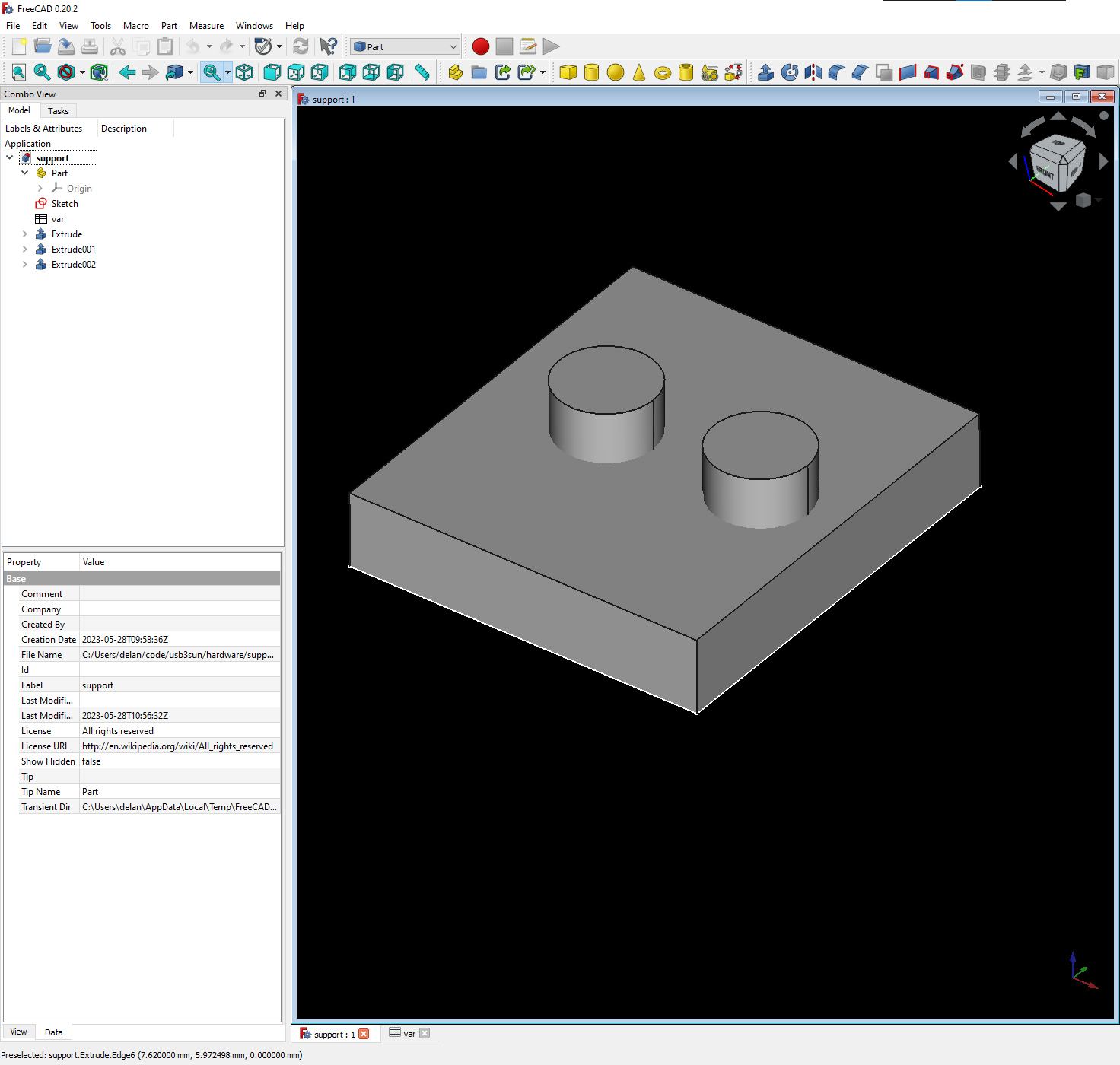
was not a panacea either.
the documentation is pretty lacking, so i had to rely on forum posts to answer basic questions like “how do you define a constant?” or “why can’t i extrude this face?”. and the latter didn’t even really help, because it was actually about scripting freecad with python.
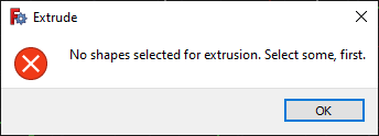
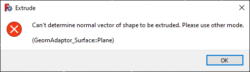
the extrude tool took me a while to figure out. i wasn’t able to just extrude the shapes i drew in the sketcher, because i first needed to “make face from wires”. due to a minor ui oversight, i wasn’t able to use variables in the length until after extruding with some arbitrary length. i also needed to punch in direction vectors by hand, which was surprising given that all of the points in my sketch were coplanar.
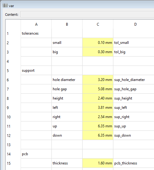
one thing that’s fun about freecad is how you define constants. unlike “change parameters” in fusion 360 — not to be confused with “edit parameters” in freecad, which is a settings editor — they implemented a whole-ass spreadsheet feature, which means you can organise your constants and format your flavour text to your heart’s content, or even split your constants across multiple spreadsheets!
that said, i feel like parameters in fusion 360 get you 70% of the way for like 20% of the effort. parameters can still refer to other parameters, and you can still organise your constants by giving them prefixes and comments, and you don’t have to type “<<Spreadsheet001>>.” before everything, so overall those seem more ergonomic.
next steps
usb3sun is more or less done, but there are still a few improvements we can make.
changing the values of the led resistors from 200R to 680R will reduce their luminous intensity from ~80% down to 15% (relative to 20mA), which should be a lot more comfortable to look at without needing modification during assembly. note that every rev A1 unit will ship with its leds modified in this way to limit their brightness appropriately.
the microcontroller can toggle SPOWER with a low-side mosfet switch, but it can’t yet read the state of SPOWER, so we can’t send the make (30h) and break (B0h) codes for power when the “hard” power key is pressed.
many of the parts on the bill of materials are considered “extended parts” by jlcpcb, which incur extra fees because someone has to physically load a reel into the pick-and-place machine. finding alternative “basic parts”, which are always kept loaded, would reduce the cost of making these adapters.
it’s difficult for the end user to update the firmware, because the micro-usb port isn’t physically accessible after assembly, so you need a picoprobe and debug tooling. there are three ways we can make this easier, in ascending order of effort:
-
adding another micro-usb port — the pico has test points for the usb port on its underside, which we can line up with small plated holes and fill them with solder. we would need to reroute D1+ and D1−, and it might complicate the routing a bit.
-
over-the-air updates — we can load a firmware update over UART0, or even easier, from a usb mass storage device. this wouldn’t require any hardware changes, but i have no idea how well this would work in practice, plus you wouldn’t be able to use this if the existing firmware is hosed.
-
embedding the rp2040 directly — we can “inline” the microcontroller and everything it needs into the pcb, eliminating the pico and allowing us to move the micro-usb port anywhere we want. this would probably make the adapter cheaper and easier to assemble, but redrawing the schematics and pcb layout would take me at least 30–50 hours, which is only worth doing if i sell more than like 3–5 units.
if you think you’ll find usb3sun useful, and you’re ok with the limitations of rev A1, consider buying one on tindie! we’ve already sold two three, but there’s currently one in stock and one being assembled. after those, we’ll need to order and assemble another run.
did you love this? hate this? have any questions or comments? please let me know in the comments below, or on mastodon or twitter!